
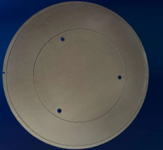
SSIC SEMICONDUCTOR COMPONENTS
Precision that holds through the process.
Dense sintered silicon carbide for wafer holding, process carriers and lightweight equipment structures. Review the material grade, contact geometry and thermal conditions together.
The contact surface is only the beginning.
Dense SSIC chucks use designed holes or surface features. They differ from porous-ceramic chucks that draw vacuum through interconnected pores.
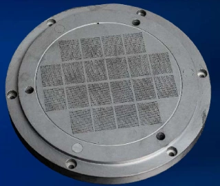
Dense-hole vacuum chuck
A representative design has 6,400 holes. Hole layout, contact area and vacuum connections are confirmed against the equipment drawing.
Pin and double-sided thin chucks
Examples include 10,000 pins on one face and a 1.2 mm double-sided chuck with 10,000 pins per face. These are separate product examples.
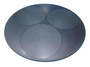
PVD process carrier
Recesses, wafer pockets and mounting features are reviewed around wafer size, coating conditions and equipment interfaces.
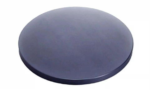
CMP carrier
Contact surfaces, geometry and cleaning requirements are evaluated for the intended polishing equipment.
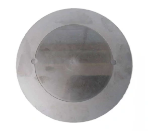
RTP / RTA carrier
A documented application uses 1,100°C for 60 seconds with nitrogen cooling. Heating, cooling and acceptance conditions require project review.
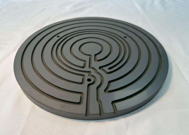
Channels and diffusion bonding
Channel layouts and lightweight back structures can be reviewed together with diffusion-bonded assembly, leak testing and cleaning.
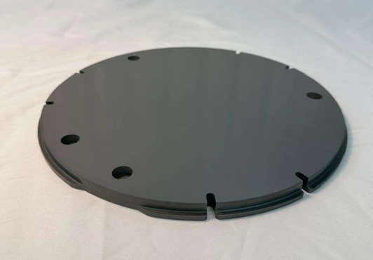
Bonding press plate
Flat contact surfaces, hole positions and alignment datums are defined from the equipment assembly and inspection plan.
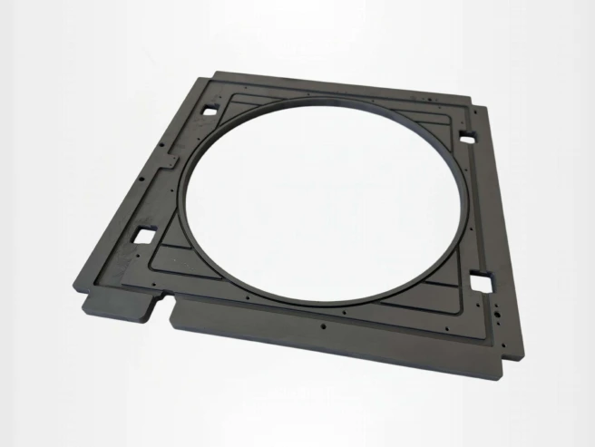
Lightweight structural frame
Frames and hollow structures balance stiffness, weight and mounting requirements for precision equipment.
Match the material to the thermal and mechanical load.
The columns below represent three material grades, not three universal part specifications.
| Property | Grade A | Grade B | Grade C |
|---|---|---|---|
| SiC content | ≥99% | ≥99% | ≥96% |
| Density (g/cm³) | ≥3.10 | >3.10 | ≥3.05 |
| Elastic modulus (GPa) | ≥410 | >420 | >400 |
| Thermal conductivity at 25°C (W/m·K) | 180 | 125 | 110 |
| CTE, 25–500°C (×10⁻⁶/K) | 4.0 | 4.0 | 4.2 |
| Four-point bending at 25°C (MPa) | ≥380 | ≥420 | ≥240 |
Values come from material test specimens. They do not directly establish performance for finished parts of different sizes, geometries or surface conditions. Grade A/B/C are comparison labels; confirm the actual grade and acceptance method before ordering.
Define the interface before setting the inspection plan.
- Review wafer size, contact areas, holes, channels and mounting datums from the drawing.
- Select a material grade and assess forming, sintering, machining and bonding where required.
- Agree dimensional inspection, surface requirements, leak checks and cleaning before acceptance.
For an assessment, share 2D/3D drawings, material, quantity, critical tolerances, temperature, atmosphere or chemicals, vacuum requirements and cleanliness targets.
Discuss an SSIC component ↗START A PROJECT
Let’s manufacture what comes next.
Share your design, application or manufacturing challenge.
Talk to our team↗